


Weekend Long Read: China’s Chipmaking Breakthrough Too Good to Be True
Science writer Wang Jie sets the record straight on much-talked-about online reports that Chinese scientists have independently developed the most advanced tech for producing semiconductors

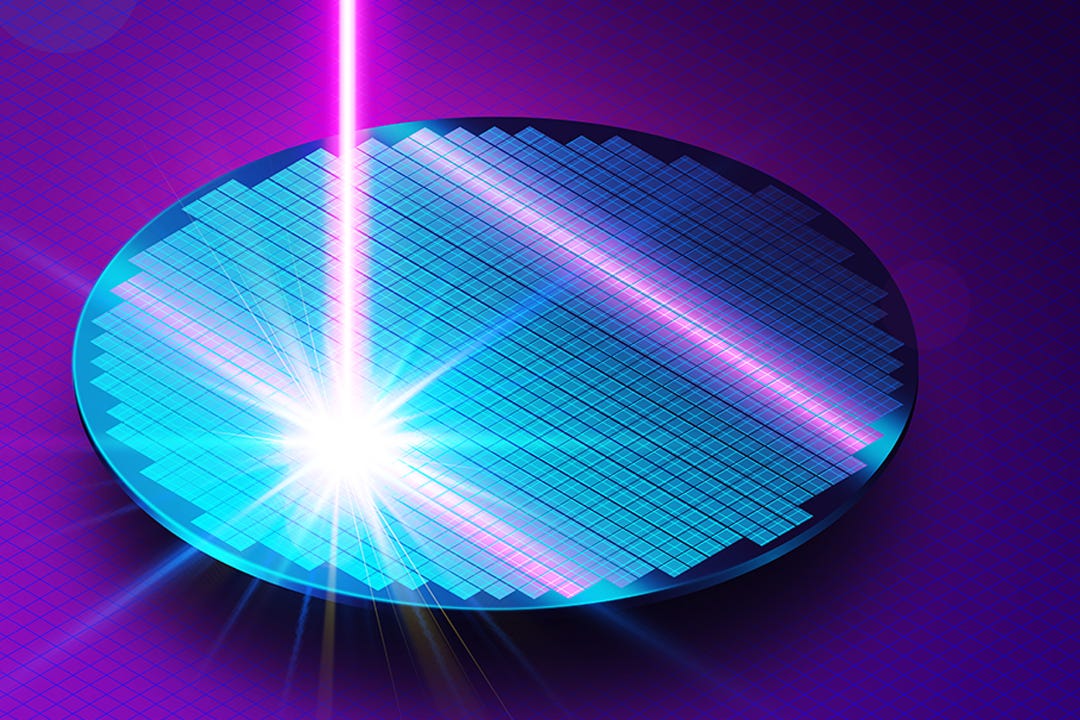
The world’s most advanced lithography machines utilize extreme ultraviolet light to produce the world’s most powerful microchips. Photo: VCG
The Chinese internet has been abuzz recently about news of a breakthrough by Chinese scientists developing an ultra-deep ultraviolet light source for photolithography — the key process for making semiconductors. The furor was exacerbated by claims that construction of a lithography machine factory is underway in Xiongan, near Beijing.
As a science writer and academic, many people have asked me to validate this news. So let’s set the record straight: The principle of this new light source is indeed real, but it was only proposed back in 2010 — the technology is still in the proof-of-concept phase and is at least 15 to 20 years away from practical application.
Bizarrely, the source of the recent excitement was a research paper published by Tsinghua University scientists more than two years ago. Why it suddenly caught the public eye is unclear. As for the claims regarding the Xiongan factory, they are mere exaggerations.
In a nutshell: no country will be able to independently produce a lithography machine at the most advanced global standard for decades. They are the most precise and intricate apparatus that humankind has ever crafted.
And to understand the significance of these machines you needn’t look further than your everyday gadgets, from laptops and tablets to smartphones and cars — they all run on chips, which are all products of lithography.
Semiconductor sophistication is measured in nanometers, indicating the size of the transistors — the smaller they are the more can fit onto a chip. For instance, the recent launch of Huawei’s new Mate 60 Pro smartphone was met with much fanfare because of speculation that it boasts a 7 nanometer (nm) chip made by China’s very own Semiconductor Manufacturing International Corp.
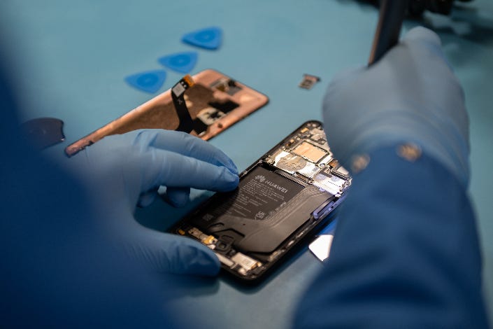
A specialist disassembles a Huawei Mate 60 Pro smartphone on Sept. 3. Since the phones launch, speculation has been rampant that the device uses a 7-nanometer processor. Photo: VCG
Chips are etched onto silicon wafers using lasers. The smaller you wish to etch, the shorter the wavelength of the laser needed. The world’s most advanced lithography machines utilize extreme ultraviolet (EUV) light, with a wavelength of 13.5 nm.
The Chinese scientists have supposedly created a new source for EUV light.
Originally developed by a U.S. company, which has since been acquired by Netherlands-based ASML Holding NV, EUV machines can produce 7 nm, 5 nm or even finer chips.
One notch below EUV is deep ultraviolet (DUV) light, which has a wavelength of 193 nm. Remarkably, the 7 nm Kirin 9000s chip in Huawei’s latest phone was produced using DUV, demonstrating the feasibility of etching 7 nm transistors with a 193 nm wavelength through a method known as multiple patterning. Currently, only a handful of global players, including ASML, Japan’s Canon Inc. and Nikon Corp., and Taiwan Semiconductor Manufacturing Co. Ltd., have mastered DUV technology.
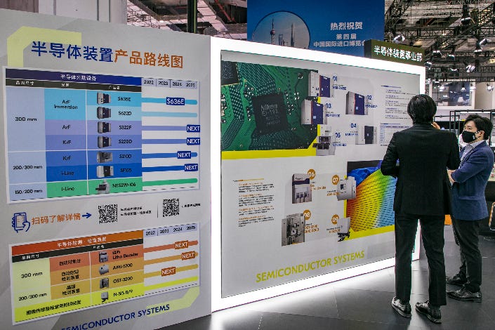
Visitors check out Nikon’s lithography machine booth at the China International Import Expo in Shanghai in November 2021. Photo: VCG
Keep reading with a 7-day free trial
Subscribe to Caixin Global China Watch to keep reading this post and get 7 days of free access to the full post archives.